
ADC and Analog Sensor Interfacing
So far your board has only seen the world as 0 or 1. In this lab you use the STM32's analog-to-digital converter (ADC) to measure real voltages: a potentiometer and a light-dependent resistor (LDR). The readings are shown live on the I²C LCD from Experiment 2.
Objectives
- Understand ADC principles: sampling, resolution and conversion time.
- Configure the STM32F4 ADC in STM32CubeIDE and read it by polling.
- Interface analog sensors (a potentiometer and an LDR) with the microcontroller.
- Display sensor readings on the LCD in real time.
Builds on Experiment 2
You reuse the LCD wiring, the I²C configuration and the LCD16x2_I2C library from Experiment 2. The keypad is not needed.
Pre-Lab
- Review the ADC basics in the Background below.
- Study the code and the ADC configuration in Step 2 and Step 5.
- With the ADC settings used in this lab (12-bit, 144-cycle sampling time, ADC clock = PCLK2 ÷ 4), what is the total conversion time on your board? Use the conversion time formula.
Background
ADC basics
Real-world signals — sound, light, temperature, motion — are analog: they vary smoothly over time. Sensors and transducers convert them into an equivalent voltage, but an embedded system only understands 0s and 1s. An analog-to-digital converter translates that voltage into a digital number the program can process.
Sampling
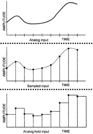
To process an analog signal digitally, it is turned into a series of discrete values. Sampling means measuring the signal at regular intervals, the sampling rate. By the Nyquist–Shannon theorem, the sampling rate must be at least twice the highest frequency in the signal to avoid aliasing.
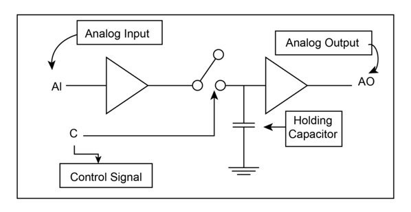
Between samples, a sample-and-hold circuit keeps the input voltage steady so the converter has a fixed value to work on.
Resolution
The ADC output is a binary number, and its number of bits n is the resolution. An n-bit ADC divides the input range into 2ⁿ levels; the 3-bit example below has only 8.
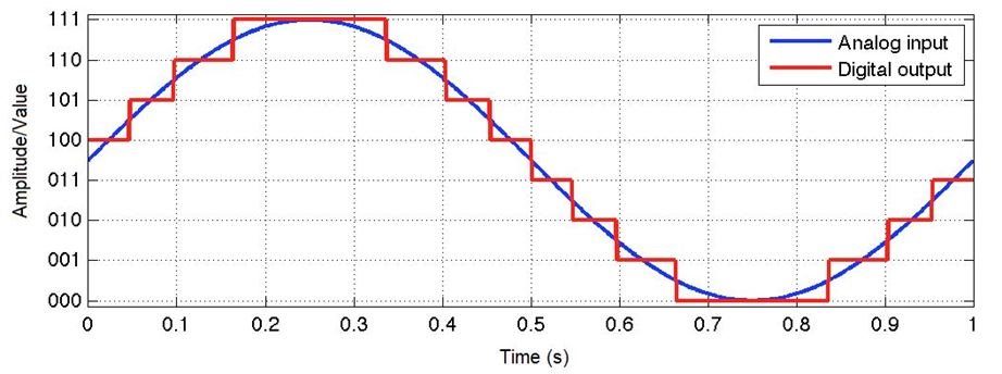
The digital output for an input voltage is:
ADC output = round( Vin / Vref × (2ⁿ − 1) )where Vin is the input voltage, Vref the ADC reference voltage and n the resolution in bits.
Example: a 12-bit ADC with Vref = 3.3 V and Vin = 1 V:
ADC output = round( 1 / 3.3 × 4095 ) = round(1240.9) = 1241Going the other way — from a reading back to volts — is what your program does: Vin = reading × Vref / 4095.
The STM32F4 ADC
The STM32F4 ADC is a successive approximation converter. It has up to 19 multiplexed channels: 16 external pins, two internal sources and the VBAT channel. Conversions run in single, continuous, scan or discontinuous mode, and the result lands left- or right-aligned in a 16-bit data register.
- Resolution is configurable: 12, 10, 8 or 6 bits.
- There are up to three ADCs (ADC1, ADC2, ADC3) on the APB2 bus, so they take their clock from PCLK2.
- APB2 is too fast for the ADC, so a dedicated prescaler (÷2, ÷4, ÷6, ÷8) divides it down. The ADC clock must not exceed 36 MHz — see the ADC characteristics table in your chip's datasheet.
- Sampling time is programmable per channel: 3, 15, 28, 56, 84, 112, 144 or 480 ADC clock cycles. Longer sampling gives the internal capacitor more time to charge, which matters for high-impedance sources such as a voltage divider.
Conversion time
The total time from the start of sampling to a ready result is:
Total conversion time = sampling time + data conversion timeThe data conversion is the successive-approximation step, and it takes as many ADC clock cycles as the resolution: 12 cycles for 12 bits.
Example: with a 21 MHz ADC clock and the shortest sampling time (3 cycles), a 12-bit conversion takes
Total conversion time = (3 + 12) cycles / 21 MHz ≈ 0.71 µsWhy CubeMX says "12 bits (15 ADC Clock cycles)"
CubeMX quotes the conversion time including the minimum 3-cycle sampling time. The formula above is the same thing: 3 + 12 = 15.
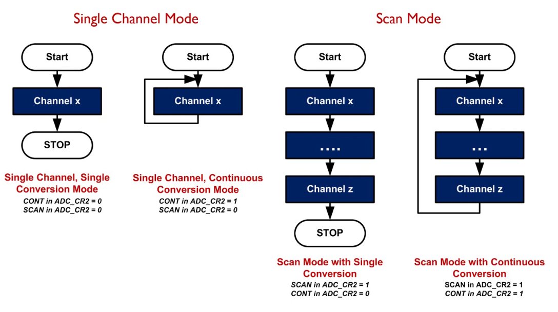
Conversion modes
| Mode | What happens |
|---|---|
| Single channel, single conversion | Convert one channel once, then stop. |
| Single channel, continuous | Convert one channel over and over. |
| Scan, single conversion | Convert a list of channels once each, then stop. |
| Scan, continuous | Convert the list of channels over and over. |
This lab uses only single channel, single conversion. To read several sensors, the program points the ADC at each channel in turn.
Regular and injected channels
The channels can be organised into two groups: regular and injected. Injected conversions can interrupt the regular sequence, like a high-priority interrupt. This lab uses only regular channels, read by polling.
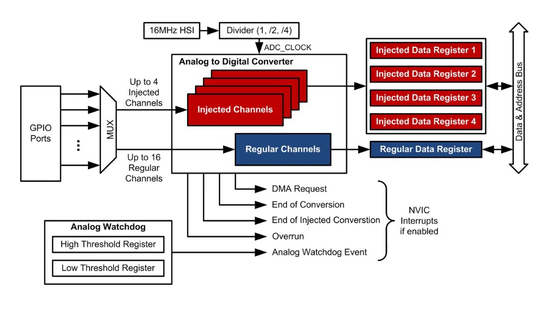
The figure is generic across STM32 families; on the F4, the ADC clock comes from PCLK2 through the prescaler described above, not from the HSI.
Internal channels
Besides the pins, ADC1 can measure three internal signals, useful for monitoring and calibration:
| Channel | Signal | HAL name |
|---|---|---|
| Temperature sensor | Die temperature. ADC1_IN16 on the F407; ADC1_IN18 (shared with VBAT) on the F411. | ADC_CHANNEL_TEMPSENSOR |
| VREFINT | A fixed internal reference of about 1.21 V. ADC1_IN17. | ADC_CHANNEL_VREFINT |
| VBAT | The backup battery voltage, divided internally. ADC1_IN18. | ADC_CHANNEL_VBAT |
These channels exist only on ADC1. This lab uses VREFINT to measure the real supply voltage — see Why measure VDDA?.
Light-dependent resistor (LDR)
An LDR, or photoresistor, is a resistor whose resistance drops as light increases. In darkness it can be several hundred kΩ; in bright light it falls to a few hundred ohms or lower. LDRs are used for automatic lighting, camera light meters and detecting objects that pass between a light source and the sensor.
The microcontroller cannot measure resistance directly, so the LDR goes in a voltage divider with a fixed resistor, turning the change in resistance into a change in voltage:
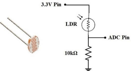
With the LDR on top and 10 kΩ to ground, more light means a lower LDR resistance and therefore a higher voltage at the ADC pin:
V(ADC) = 3.3 V × 10 kΩ / (R(LDR) + 10 kΩ)Materials and Equipment
- STM32F4 evaluation board and USB cable
- Breadboard and jumper wires
- 16×2 LCD with PCF8574 I²C adapter
- Potentiometer (e.g. 10 kΩ)
- LDR (photoresistor) and a 10 kΩ resistor
- An LED and a current-limiting resistor (for the Task)
Relevant HAL APIs
Single channel, single conversion mode needs four calls:
HAL_ADC_Start(&hadc1);                  /* Start a conversion */
HAL_ADC_PollForConversion(&hadc1, 100); /* Wait (poll) until it finishes, 100 ms timeout */
HAL_ADC_GetValue(&hadc1);               /* Read the converted value */
HAL_ADC_Stop(&hadc1);                   /* Stop the ADC */
To change which channel is converted, fill an ADC_ChannelConfTypeDef and pass it to HAL_ADC_ConfigChannel(&hadc1, &sConfig).
Activity
Write firmware that reads a potentiometer and an LDR through the ADC and shows both voltages on the LCD in real time.
Step 1: Wire the hardware
- Connect the LCD exactly as in Experiment 2: SCL → PB6, SDA → PB7, +5 V and GND to the adapter board.
- Build the LDR voltage divider from the figure above: LDR from 3.3 V to the midpoint, 10 kΩ from the midpoint to GND. Connect the midpoint to PA6.
- Connect the potentiometer: one end to 3.3 V, the other to GND, and the middle pin (wiper) to PA4.
| Signal | Pin | ADC channel | Nucleo-F411 header |
|---|---|---|---|
| LDR divider | PA6 | ADC1_IN6 | D12 |
| Potentiometer | PA4 | ADC1_IN4 | A2 |
Analog inputs take 3.3 V at most
Feed the sensors from the board's 3.3 V pin, not 5 V. A pin in analog mode is not 5 V tolerant, and anything above VDDA reads as 4095 at best and damages the pin at worst. The LCD is the only thing on 5 V in this lab.
Step 2: Configure the peripherals
Create the project. Follow Setup Guide → Create a lab project with the name
Exp3_ADC, including the maximum-frequency clock configuration.Configure I²C for the LCD. Enable I2C1 in Standard Mode at 100 kHz on PB6/PB7, as in Experiment 2.
Enable the ADC channels. Under Analog → ADC1, tick IN4, IN6 and Vrefint Channel.
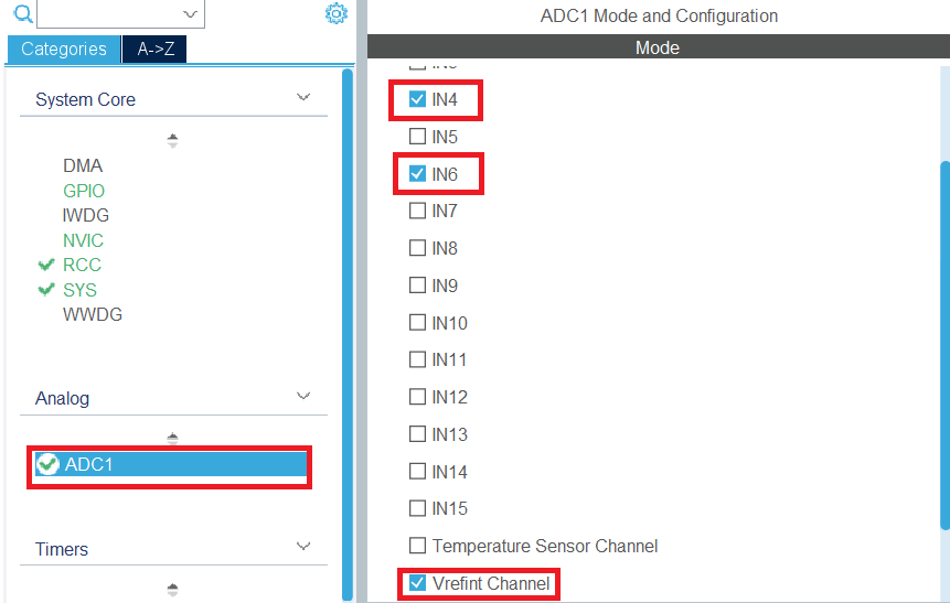
CubeMX switches PA4 and PA6 to ADC1_IN4 and ADC1_IN6 (analog mode) in the pinout view.
Set the ADC parameters. In Parameter Settings, keep the defaults — independent mode, PCLK2 divided by 4, 12-bit resolution, right alignment, scan / continuous / discontinuous disabled, one regular conversion — and set the Sampling Time of rank 1 to 144 Cycles.
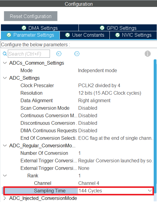
The rank 1 channel chosen here does not matter much: the program reconfigures the channel before every reading.
Generate the code.
Step 3: Enable float support in printf
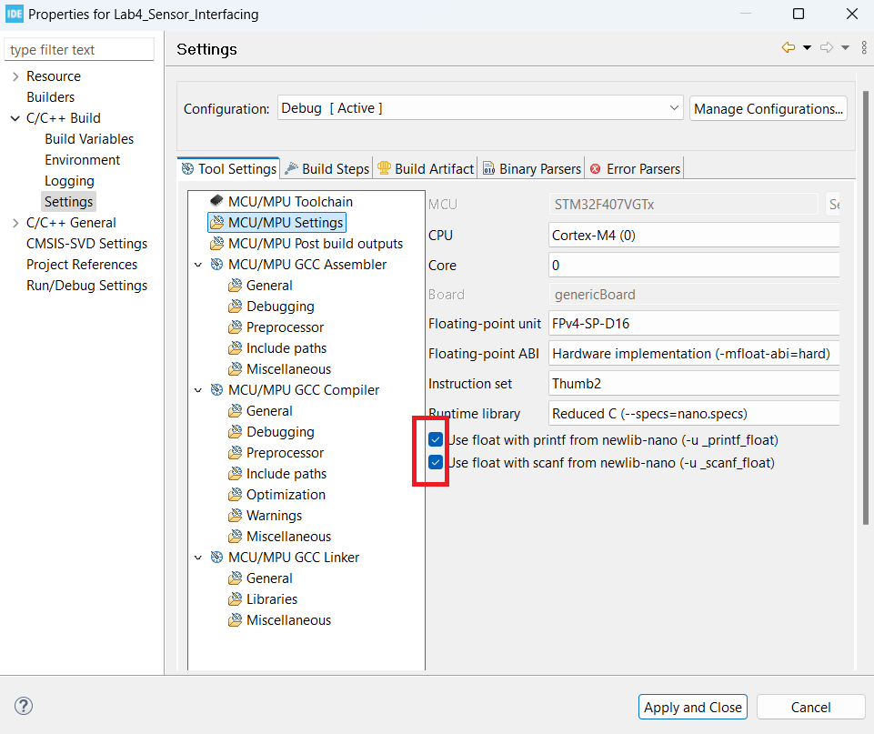
The program formats voltages with snprintf("%.3f", …). The default C library in CubeIDE (newlib-nano) leaves out float formatting to save flash, so without this step you get an empty string.
Open Project → Properties → C/C++ Build → Settings → Tool Settings → MCU/MPU Settings and tick Use float with printf from newlib-nano (-u _printf_float).
Step 4: Add the LCD library
Copy the LCD library from Experiment 2 — LCD16x2_I2C.h into Core/Inc/ and LCD16x2_I2C.c into Core/Src/. Then add the includes, constants and prototypes to main.c:
/* USER CODE BEGIN Includes */
#include <stdio.h>
#include <LCD16x2_I2C.h>
/* USER CODE END Includes */

/* USER CODE BEGIN PD */
#ifndef VREFINT_CAL_ADDR
#define VREFINT_CAL_ADDR ((uint16_t *)0x1FFF7A2AU) /* factory VREFINT reading, taken at VDDA = 3.3 V */
#endif
#define VREFINT_CAL_VREF 3.3f
#define ADC_FULL_SCALE   4095.0f                    /* 2^12 - 1 for a 12-bit result */
/* USER CODE END PD */

/* USER CODE BEGIN PFP */
uint32_t ADC_Get_Value(ADC_HandleTypeDef *hadc, uint32_t channel);
float    ADC_Get_Vdda(void);
void     LCD_displayFloat(float value);
/* USER CODE END PFP */
VREFINT_CAL_ADDR points at a value ST measured on every chip at the factory: the VREFINT reading taken with VDDA at exactly 3.3 V. The #ifndef guard is there because newer HAL versions already define it.
Step 5: Write the ADC functions
/* USER CODE BEGIN 4 */
/* Point ADC1 at one channel and convert it once (single channel, single conversion). */
uint32_t ADC_Get_Value(ADC_HandleTypeDef *hadc, uint32_t channel)
{
    ADC_ChannelConfTypeDef sConfig = {0};
    uint32_t value = 0;

    sConfig.Channel = channel;
    sConfig.Rank    = 1;
    /* VREFINT must be sampled for at least 10 us (datasheet), so it gets the longest time */
    sConfig.SamplingTime = (channel == ADC_CHANNEL_VREFINT) ? ADC_SAMPLETIME_480CYCLES
                                                             : ADC_SAMPLETIME_144CYCLES;
    if (HAL_ADC_ConfigChannel(hadc, &sConfig) != HAL_OK)
    {
        Error_Handler();
    }

    HAL_ADC_Start(hadc);
    if (HAL_ADC_PollForConversion(hadc, 100) == HAL_OK)   /* wait up to 100 ms */
    {
        value = HAL_ADC_GetValue(hadc);
    }
    HAL_ADC_Stop(hadc);

    return value;
}

/* Measure the real analog supply (VDDA) from the internal reference. */
float ADC_Get_Vdda(void)
{
    uint32_t vrefint     = ADC_Get_Value(&hadc1, ADC_CHANNEL_VREFINT);
    uint16_t vrefint_cal = *VREFINT_CAL_ADDR;

    if (vrefint == 0)
    {
        return VREFINT_CAL_VREF;    /* conversion failed: assume the nominal 3.3 V */
    }
    return VREFINT_CAL_VREF * (float)vrefint_cal / (float)vrefint;
}

/* Show a float with 3 decimals at the cursor, e.g. "1.652". */
void LCD_displayFloat(float value)
{
    char text[12];
    snprintf(text, sizeof text, "%.3f", value);
    LCD_displayText(text);
}
/* USER CODE END 4 */ADC_Get_Valuedoes one single-channel, single conversion: it selects the channel withHAL_ADC_ConfigChannel, then runs the four calls from Relevant HAL APIs.valuestarts at 0, so a timed-out conversion returns 0 instead of garbage.ADC_Get_Vddareads VREFINT and compares it with the factory calibration to work out the real supply voltage. It is explained in Why measure VDDA?.LCD_displayFloatformats a float with three decimals and prints it at the cursor.
VREFINT needs a long sampling time
The datasheet requires VREFINT to be sampled for at least 10 µs. At 144 cycles of a 21–25 MHz ADC clock, that is only about 6–7 µs, so the reading would be off. That is why ADC_Get_Value switches to 480 cycles for that one channel.
Step 6: Put it together
In main, after the generated init calls, initialise the LCD and show a start-up message. In the loop, measure VDDA, read both channels, convert each reading to volts and print it.
int main(void)
{
    HAL_Init();
    SystemClock_Config();
    MX_GPIO_Init();
    MX_I2C1_Init();
    MX_ADC1_Init();

    /* USER CODE BEGIN 2 */
    LCD_init();
    LCD_clear();
    LCD_setCursor(0, 0);
    LCD_displayText("LAB3 ADC");
    HAL_Delay(1000);
    LCD_clear();
    /* USER CODE END 2 */

    /* USER CODE BEGIN WHILE */
    while (1)
    {
        float vdda = ADC_Get_Vdda();                         /* the real full-scale voltage */

        uint32_t ldr = ADC_Get_Value(&hadc1, ADC_CHANNEL_6); /* PA6: LDR divider */
        uint32_t pot = ADC_Get_Value(&hadc1, ADC_CHANNEL_4); /* PA4: potentiometer */

        LCD_setCursor(0, 0);
        LCD_displayText("LDR:");
        LCD_setCursor(0, 10);
        LCD_displayFloat(ldr * vdda / ADC_FULL_SCALE);
        LCD_displayText("V");

        LCD_setCursor(1, 0);
        LCD_displayText("POT:");
        LCD_setCursor(1, 10);
        LCD_displayFloat(pot * vdda / ADC_FULL_SCALE);
        LCD_displayText("V");

        HAL_Delay(200);
    }
    /* USER CODE END WHILE */
}
Build the project and flash it. Turn the potentiometer and cover the LDR with your hand, and watch both voltages change.
Why measure VDDA?
Converting a reading to volts needs the ADC's reference voltage: Vin = reading × Vref / 4095. On these boards the reference is the analog supply VDDA, nominally 3.3 V — but the regulator is never exact.
In battery-powered products the problem is worse: VDDA often comes straight from the battery and drops as it discharges. Assume 3.3 V and every voltage you calculate drifts with it.
There are two fixes:
- Hardware: feed VREF+ from a precise external reference.
- Software: measure a voltage you already know. VREFINT is a fixed internal reference, and ST stores its reading at VDDA = 3.3 V in
VREFINT_CAL. If VDDA drops, the same VREFINT now reads higher, so
VDDA = 3.3 V × VREFINT_CAL / VREFINT readingThat is exactly what ADC_Get_Vdda() computes (the calculation comes from the reference manual), and the program uses it in place of a fixed 3.3 V.
Common problems
| Symptom | Cause and fix |
|---|---|
Voltages show as blank or just V | Float formatting is off. Tick Use float with printf (Step 3), then Project → Clean and rebuild. |
| Reading stuck at 0 | Wrong pin or channel, or the sensor is not powered. Check PA4/PA6 are set to ADC1_IN4/IN6 in the pinout view. |
| Reading stuck at 4095 | The input is at or above VDDA, or the divider's bottom resistor is missing. |
| Readings jump around | A loose breadboard wire, or the sampling time is too short for the source. Keep 144 cycles for the pins. |
| VDDA shows a strange value (e.g. 2.8 V or 4 V) | The VREFINT sampling time is too short. Check ADC_Get_Value uses 480 cycles for ADC_CHANNEL_VREFINT, and that Vrefint Channel is ticked. |
Build fails: implicit declaration of ADC_Get_Value | The prototypes are missing from USER CODE BEGIN PFP. |
| LCD blank | See the Experiment 2 common problems. LCD_init() must come after MX_I2C1_Init(). |
Post-lab questions
- What is the total conversion time of each reading in this lab (144-cycle sampling, 12-bit, your board's ADC clock)? How long does reading VREFINT take at 480 cycles?
- What is the smallest voltage change the 12-bit ADC can detect with a 3.3 V reference? What about at 8 bits?
- Why does the program reconfigure the channel before every conversion instead of using scan mode?
- Swap the LDR and the 10 kΩ resistor in the divider. What happens to the voltage when the light increases?
- Why is measuring VDDA through VREFINT more accurate than assuming 3.3 V?
Task
Write logic that monitors the LDR reading. If it indicates low light, turn on an LED; otherwise the LED stays off. The LED must not flicker because of small variations in the LDR reading.
For the task
A single threshold flickers when the reading sits right on it, because the noise pushes it back and forth. Use two thresholds instead — turn the LED on below the lower one and off above the higher one, and leave it as it is in between. This is called hysteresis. Measure the voltages in the dark and under the room light first, then pick your thresholds.
Things to try
- Read the internal temperature sensor (
ADC_CHANNEL_TEMPSENSOR, tick Temperature Sensor Channel in CubeMX) and convert it to °C with the formula in the reference manual's Temperature sensor section. It also needs a long sampling time. - Change the resolution to 8 bits and compare how smoothly the potentiometer voltage changes.