
Board Pinout
One page to check before you wire anything: what each board already connects to its pins, which pins are safe to use, and which pins every experiment uses. The board user manuals have the full details: UM1472 (F407 Discovery) and UM1724 (Nucleo-64).
F407 Discovery headers
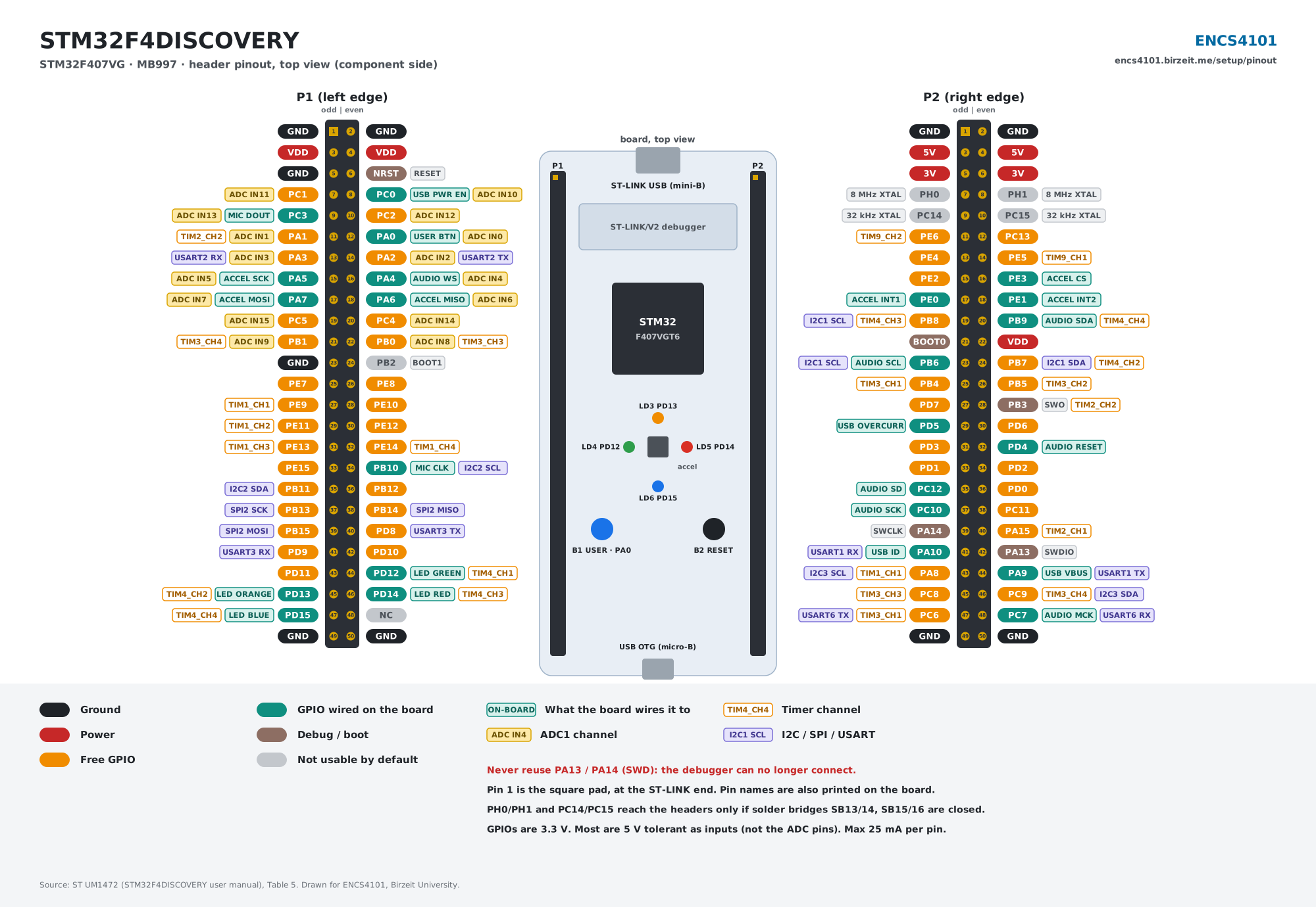
Top view (component side)
Use this when you look at the board the normal way up, LEDs facing you.
Bottom view (solder side)
Use this when you wire from underneath, for example with the board upside down on a breadboard. The board is flipped left-to-right, so P2 is on the left, P1 is on the right, and the even pins are in the left column of each header.
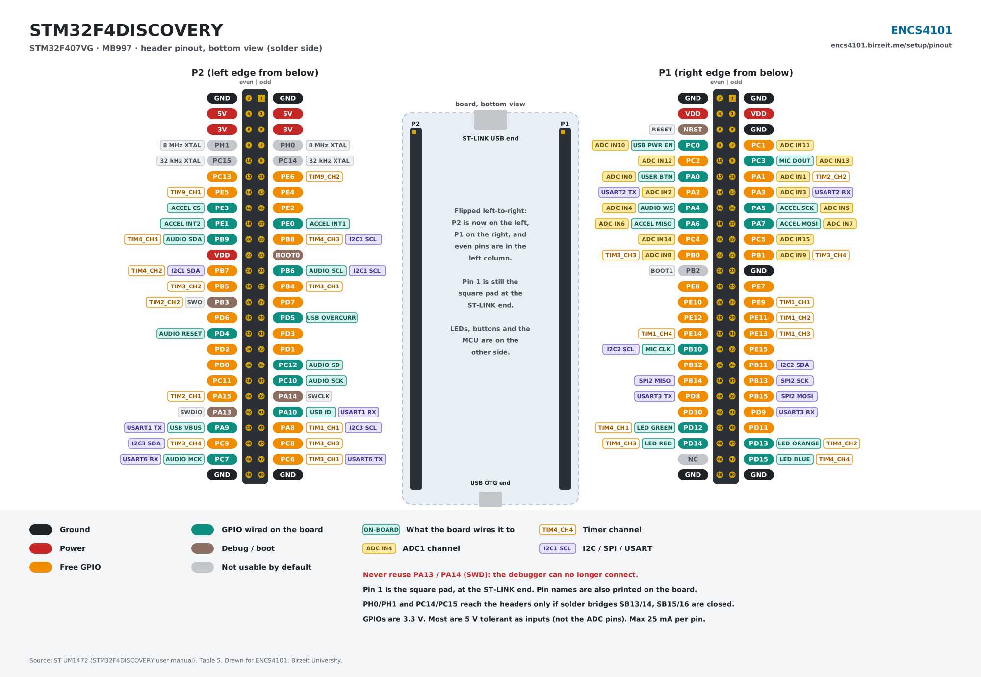
Click a drawing to open it full size, or download the top view and bottom view. Drawn from ST's UM1472, Table 5.
F411 Nucleo-64 headers
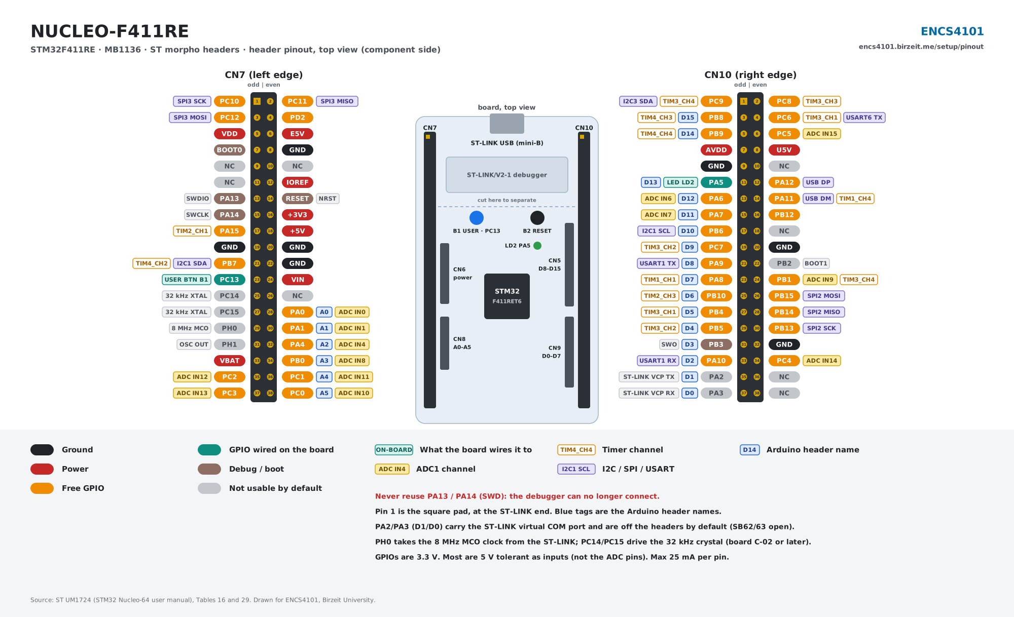
These are the two long ST morpho headers (CN7 and CN10). Every pin on the short Arduino headers is also on a morpho pin; the blue tags give its Arduino name (A0–A5, D0–D15).
Top view (component side)
Bottom view (solder side)
Flipped left-to-right: CN10 is on the left, CN7 is on the right, and the even pins are in the left column of each header.
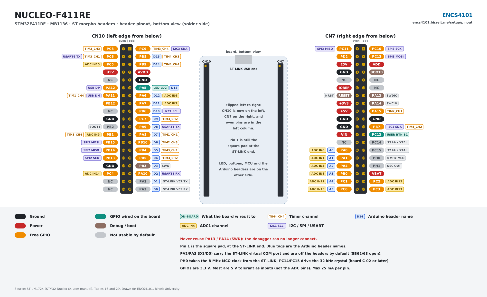
Download the top view and bottom view. Drawn from ST's UM1724, Tables 16 and 29, with the solder-bridge defaults of board revision MB1136 C-02 or later. All four drawings are generated by python3 scripts/draw-pinouts.py.
Official pinout documents
| Board | Header map | Schematic |
|---|---|---|
| F407 Discovery (MB997) | UM1472: Extension connectors table (P1/P2 pin for every MCU pin) and the Top layout figure | MB997 schematic |
| F411 Nucleo-64 | UM1724: Arduino and Morpho connectors figures for NUCLEO-F411RE | Board page (schematic pack under Documentation) |
On the Discovery, pin 1 of P1 and P2 is the square pad at the ST-LINK end, and every pin name is also printed on the board next to its pin.
Never use PA13 / PA14
They are the SWD debug pins on both boards. Assign them to anything else and the debugger can no longer connect. See Setup Guide → Know your board.
Pins used in each experiment
| Experiment | Signal | F407 Discovery | F411 Nucleo-64 |
|---|---|---|---|
| 1. GPIO | 4 LEDs, 1 button | Your choice, ideally all on one port (e.g. PD12–PD15) | Your choice, ideally all on one port |
| 2. LCD and Keypad | LCD SCL / SDA (I2C1) | PB6 / PB7 | PB6 / PB7 (D10 / Morpho CN7) |
| Keypad rows, columns | 8 free GPIOs, your choice | 8 free GPIOs, your choice | |
| 3. ADC | Potentiometer | PA4 (ADC1_IN4) | PA4 (A2) |
| LDR divider | PA6 (ADC1_IN6) | PA6 (D12) | |
| 4. Timers | LED, TIM4_CH4 | PD15 (on-board blue LED) | PB9 (D14) |
| Potentiometer, LCD | PA4, PB6 / PB7 | PA4, PB6 / PB7 | |
| 5. DC Motor and PWM | L298 ENA, TIM4_CH4 | PD15 (blue LED glows with the duty) | PB9 (D14) |
| L298 IN1 / IN2 | PB4 / PB5 | PB4 / PB5 (D5 / D4) | |
| User button | PA0 (on-board) | PC13 (on-board) | |
| Potentiometer, LCD | PA4, PB6 / PB7 | PA4, PB6 / PB7 |
F407 Discovery
Wired on the board
These pins already connect to something on the Discovery board. Use them for that part, or check the note before reusing them.
| Part | Pins | Note |
|---|---|---|
| Green / orange / red / blue LEDs (LD4, LD3, LD5, LD6) | PD12 / PD13 / PD14 / PD15 | Active high. PD12–PD15 are TIM4 channels 1–4. |
| User button B1 (blue) | PA0 | Active high, with an on-board pull-down. Also WKUP and TIM2/TIM5_CH1. |
| SWD debug | PA13 (SWDIO), PA14 (SWCLK), PB3 (SWO) | Never reuse PA13/PA14. PB3 only matters if you use SWV trace. |
| 8 MHz crystal (HSE) | PH0, PH1 | Not available as GPIO. |
| Accelerometer (SPI1) | PA5 SCK, PA6 MISO, PA7 MOSI, PE3 CS, PE0 / PE1 INT | |
| Audio DAC CS43L22 | PB6 SCL, PB9 SDA (I2C1); PA4 WS, PC7 MCK, PC10 SCK, PC12 SD (I2S3); PD4 reset | The LCD shares I2C1 with this chip. They have different addresses, so both work on the same bus. |
| Microphone MP45DT02 | PB10 CLK, PC3 DOUT | |
| USB OTG FS | PA9 VBUS, PA10 ID, PA11 DM, PA12 DP, PC0 power enable, PD5 overcurrent | PA9 also lights the green VBUS LED. |
| BOOT1 | PB2 | Has a resistor to GND; avoid. |
PA4 and PA6 are shared, and that is fine
Experiment 3 reads the potentiometer on PA4 and the LDR on PA6, which are also wired to the audio DAC and the accelerometer. Neither chip drives those lines while it sits idle, so the ADC readings are normal. If a reading on one of them looks wrong, move that sensor to a free ADC pin such as PA1 or PC1 and change the channel to match.
Free for your circuits
Nothing on the board connects to these, so they are the safest picks for LEDs, buttons, keypads and sensors:
| Port | Free pins |
|---|---|
| A | PA1, PA2, PA3, PA8, PA15 |
| B | PB0, PB1, PB4, PB5, PB7, PB8, PB11–PB15 |
| C | PC1, PC2, PC4, PC5, PC6, PC8, PC9, PC11, PC13 |
| D | PD0–PD3, PD6–PD11 |
| E | PE2, PE4–PE15 |
Free pins with ADC channels: PA1 (IN1), PA2 (IN2), PA3 (IN3), PB0 (IN8), PB1 (IN9), PC1 (IN11), PC2 (IN12), PC4 (IN14), PC5 (IN15).
F411 Nucleo-64
Wired on the board
| Part | Pins | Note |
|---|---|---|
| User LED LD2 (green) | PA5 (D13) | Active high. |
| User button B1 (blue) | PC13 | Active low: reads 0 when pressed. |
| ST-LINK virtual COM port (USART2) | PA2 TX, PA3 RX | Used by the UART labs. By default they go to the ST-LINK only, not to the D1/D0 header pins (solder bridges SB62/63 open). |
| SWD debug | PA13 (SWDIO), PA14 (SWCLK), PB3 (SWO) | Never reuse PA13/PA14. |
| 32.768 kHz crystal (LSE) | PC14, PC15 | Avoid. |
| 8 MHz clock from ST-LINK (MCO) | PH0 | Not available as GPIO. |
Arduino header
The Arduino-style header is the quickest way to find a pin on the Nucleo. Every other pin is on the two long Morpho headers (CN7, CN10).
| Header | Pin | Header | Pin |
|---|---|---|---|
| A0 | PA0 | D8 | PA9 |
| A1 | PA1 | D9 | PC7 |
| A2 | PA4 | D10 | PB6 |
| A3 | PB0 | D11 | PA7 |
| A4 | PC1 | D12 | PA6 |
| A5 | PC0 | D13 | PA5 (LD2) |
| D0 | PA3 (VCP RX) | D14 | PB9 |
| D1 | PA2 (VCP TX) | D15 | PB8 |
| D2 | PA10 | ||
| D3 | PB3 (SWO) | ||
| D4 | PB5 | ||
| D5 | PB4 | ||
| D6 | PB10 | ||
| D7 | PA8 |
D14 / D15 are not I2C here
On many Arduino shields D14/D15 are SDA/SCL. On this board they are PB9/PB8, and Experiments 4 and 5 put TIM4_CH4 on PB9. Keep the LCD on PB6 / PB7, as in Experiment 4.